
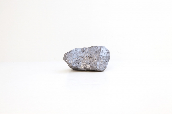
This cool, hard, lustrous rock is silicon. Silicon is one of the most ubiquitous building blocks of the material world, and it crops up in many other familiar materials. For instance, ordinary glass, silicone polymers, clays, flint and many gemstones contain silicon in their elemental makeup.
Silicon is rarely found in this pure form in nature. Instead, silicon’s affinity for other elements like oxygen and metals sees it occurring naturally in a number of minerals that together make up over 90% of the Earth’s crust. It was this affinity for other elements that prevented silicon’s isolation into its pure form until 1823, a feat which was achieved by Swedish chemist Jöns Jakob Berzelius.
A lump of silicon like this is most likely to be used in steel refining or aluminium casting. But of course, today silicon is almost synonymous with technology and electronics; Silicon Valley in California and Silicon Roundabout in London are named in homage to silicon’s central function in these industries. Indeed, some have described the current time since the late 20th Century as the Silicon Age, after the naming convention of Stone, Bronze and Iron Ages to describe the materials which dominated the – sometimes literally cutting-edge – technologies of those periods.
This historic role is all down to the fact that silicon is a semiconductor. Ordinarily, silicon is an electrical insulator, but the presence of impurities such as phosphorus, arsenic, boron or gallium mobilises carriers of electrical charge inside, turning it into an electrical conductor. Patterning different regions of a silicon wafer with different elemental additions can control the direction of flow of charge carriers, and this is the guiding principle of semiconductor devices.
Semiconductor devices were first developed in the 1870s, but the first to be based on silicon came in 1906: a silicon radio crystal detector made by American engineer Greenleaf Whittier Pickard. The 1940s and 1950s were the golden era of semiconductor research, and a cascade of breakthroughs led to a plethora of semiconductor-based devices such as amplifiers and transistors. It was the latter which would see silicon propelled to stardom.
However, at this point in history silicon’s fame was far from guaranteed. During those glorious decades of research, it was germanium which dominated the semiconductor field, rather than silicon. The simple reason was that it performed better. Silicon’s problem was that, due to a fluke in molecular bonding and the weird and wonderful world of material surfaces, dangling bonds at the surface of silicon trapped electrons which inhibited their flow, an affliction not suffered by germanium. Why, then, is it not Germanium Valley?
Silicon’s remedy was found by Egyptian engineer Mohamed M. Atalla at Bell Labs, who stabilised the surface of silicon by coating it with a layer of silicon dioxide. The dangling bonds dangled no more and this process saw silicon’s performance surpass that of germanium, and it paved the way for mass-produced silicon-based electronics. Atalla, together with his Korean colleague Dawon Kahng went on to invent the MOSFET (metal-oxide-silicon field-effect transistor) in 1959, a mass-producible silicon-based device which kick-started the silicon revolution. It is the continual miniaturising of MOSFETs which we have to thank for the exponential increase in computing power since their inception, as described by the famous Moore’s Law. They are now the most widely-manufactured device in history.
Silicon’s sensitivity to impurities means that electronics-grade silicon must be of extremely high purity material; typically, 99.9999999%. In addition to this, silicon wafers must be single crystals, meaning that the silicon atoms inside all stack up into a perfect 3D structure. Any mistakes in this structure cause charge-carrying electrons to become snagged and the performance of the device reduces. Such pristinely crystalline silicon wafers are made by the Czochralski method, a process developed by Polish chemist Jan Czochralski in 1915 after accidentally dipping his pen into molten tin instead of his inkpot, and withdrawing from it a single crystal of tin. The modern-day silicon version involves withdrawing a seed crystal of silicon from a crucible containing molten silicon at over 1400°C, which slowly solidifies onto the seed to produce a large single crystal silicon ingot. This is then sliced into thin wafers.
Sample ID: 472
Gallery
Particularities
- Selections
- Categories
- Mineral
- Curiosities
- Revolutionary | Ubiquitous
- Relationships
- Cold | Electronics | Element | Metallic | Rock | Semiconductor | Shiny | Silver
Add materials you find interesting to your own selections.
Use the  button to select a material and get started.